
China’s EUV Lithography Prototype Enters Testing Phase: A Pivotal Step Toward Semiconductor Independence
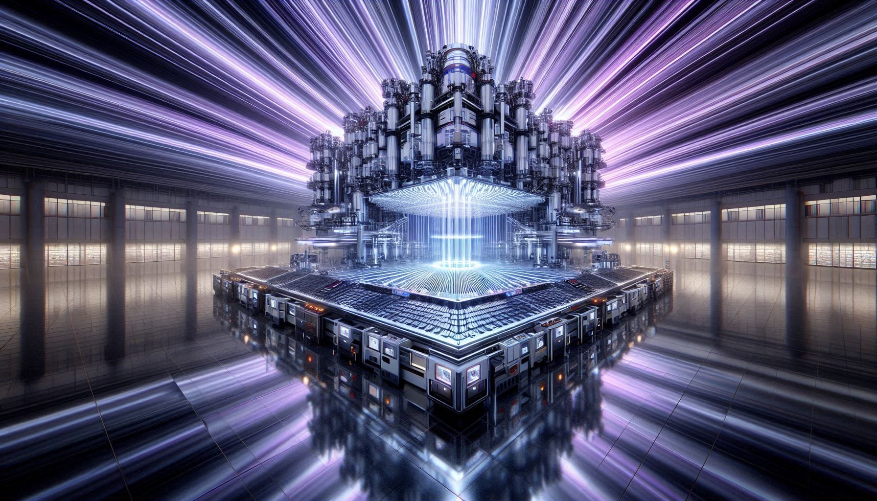
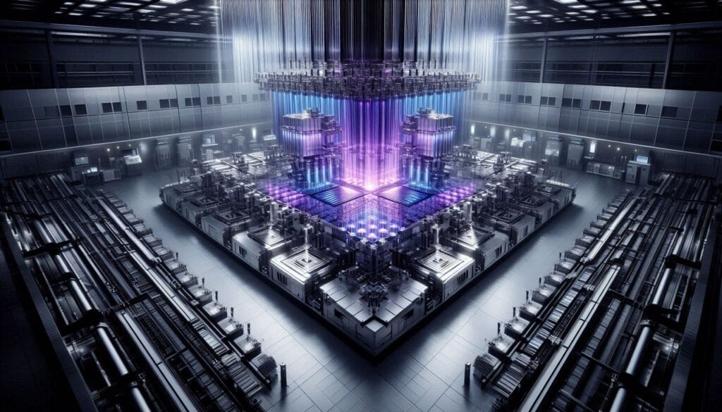
In a development that could reshape the global semiconductor landscape, reports emerged on December 17, 2025, of a working prototype of a Chinese extreme ultraviolet (EUV) lithography machine now undergoing rigorous testing. According to exclusive sources cited by Reuters, this massive prototype—occupying nearly an entire factory floor in a high-security laboratory in Shenzhen—was completed in early 2025 by a team including former engineers from ASML, the Dutch firm that has long dominated the EUV market.
This milestone represents a potential breakthrough for China in its quest for self-reliance in advanced chip manufacturing, amid ongoing U.S.-led export restrictions on critical technologies. EUV lithography is the cornerstone of producing the world’s most sophisticated semiconductors—those powering artificial intelligence, 5G networks, and cutting-edge consumer electronics. For years, ASML’s near-monopoly on EUV tools has been a chokepoint, with no machines sold to Chinese firms due to geopolitical controls.
The prototype’s testing phase signals China’s determination to challenge this dominance. While commercial viability remains years away—sources estimate functional chip production no earlier than 2030—this achievement underscores Beijing’s “Manhattan Project”-style investment in domestic innovation. As the world watches, this Chinese EUV lithography prototype could herald a new era of competition, potentially easing supply chain vulnerabilities and accelerating advancements in AI and high-performance computing.
Understanding EUV Lithography: The Heart of Modern Chipmaking
To appreciate the significance of this Chinese EUV lithography prototype, one must first grasp the technology’s complexity. Extreme ultraviolet lithography uses light with a wavelength of just 13.5 nanometers to etch intricate patterns onto silicon wafers. This enables transistors as small as 3-5 nanometers, essential for packing billions of components into a single chip.
Traditional deep ultraviolet (DUV) systems, operating at longer wavelengths, reach their physical limits around 7-10nm processes. EUV overcomes this by employing highly reflective mirrors and vacuum chambers to manipulate light that is absorbed by air. ASML’s EUV machines—each costing over $200 million and weighing hundreds of tons—represent decades of collaborative R&D involving thousands of patents.
China’s efforts have focused on two paths: reverse-engineering restricted technologies and pioneering alternatives. The Shenzhen prototype reportedly incorporates older ASML components acquired through secondary markets, combined with domestic innovations in light sources and optics. Key challenges include generating stable EUV light (often via laser-produced plasma), precise mirror coatings, and vacuum system integrity—all areas where ASML holds overwhelming advantages.
The Prototype’s Development: A Clandestine “Manhattan Project”
Sources describe the project as China’s semiconductor “Manhattan Project”—a coordinated, state-backed push involving vast resources and talent poaching. The team in Shenzhen includes ex-ASML specialists, lured by competitive incentives amid global talent wars.
Completed in early 2025, the prototype is monumental in scale, reflecting the technology’s demands: immense power requirements, sophisticated cooling, and contamination-free environments. Testing involves calibrating light source stability, pattern accuracy, and throughput—metrics where ASML’s machines achieve near-perfection.
Early indications suggest the prototype generates EUV light effectively, a hurdle many skeptics doubted China could clear independently. However, yield rates, resolution consistency, and production speed remain unproven. Analysts estimate 3-5 years for refinement, with full commercialization potentially by the early 2030s.
This aligns with broader initiatives: Shanghai Micro Electronics Equipment (SMEE) advancing DUV tools to 28nm and beyond, while institutions like Harbin Institute of Technology explore laser-induced discharge plasma (LDP) alternatives to ASML’s laser-produced plasma (LPP).
Challenges Ahead: From Prototype to Production
Despite the optimism, significant obstacles loom for this Chinese EUV lithography prototype. ASML’s ecosystem—supply chain mastery, software optimization, and field service—took decades to perfect. China’s machine, reliant on salvaged parts, may face reliability issues.
Intellectual property concerns abound: incorporating ASML components risks legal challenges, though secondary sourcing complicates enforcement. Geopolitical tensions could intensify scrutiny on global suppliers.
Moreover, EUV demands an intricate supply chain: high-purity materials, advanced lasers (often from U.S. or Japanese firms), and metrology tools. China’s domestic alternatives are progressing but lag in precision.
Testing outcomes will be pivotal. Success in patterning sub-7nm features at viable yields could enable firms like SMIC and Huawei to produce competitive AI chips, reducing dependence on TSMC and Samsung.
Global Implications: Reshaping the Semiconductor Balance
The emergence of a viable Chinese EUV lithography prototype carries profound ramifications. For the U.S. and allies, it challenges export control efficacy—designed to maintain a “generation ahead” lead in chips.
Economically, it could diversify supply chains, mitigating risks exposed during recent shortages. For AI development, indigenous EUV access might accelerate China’s progress in training massive models, narrowing gaps with Western leaders.
ASML shares dipped on the news, reflecting market jitters. Yet experts caution optimism: even if testing succeeds, scaling to commercial volumes requires billions more in investment and years of iteration.
This prototype also highlights China’s resilience. Massive funding—reportedly tens of billions annually—fuels parallel paths: multi-patterning DUV for interim gains, particle accelerators (SSMB-EUV), and solid-state lasers.
Broader Context: China’s Semiconductor Odyssey
China’s journey began with humility: lagging decades behind in the 2010s. U.S. restrictions post-2018 catalyzed the “whole-nation” approach, yielding fruits like 7nm chips via DUV ingenuity.
The EUV push involves national champions: Huawei coordinating integration, SMEE on tools, and academies on fundamentals. Investments exceed $100 billion since 2014, building ecosystems in Shenzhen, Shanghai, and Beijing.
While skeptics note past overhyped claims, this prototype’s tangible existence—verified through multiple channels—marks substantive progress.
Conclusion: A Watershed Moment with Cautious Optimism
The testing of China’s EUV lithography prototype stands as a testament to human ingenuity amid adversity. It embodies Beijing’s unyielding pursuit of technological sovereignty, potentially altering the global chip dynamics for generations.
Yet realism tempers excitement: from prototype to pervasive production lies a gauntlet of technical, economic, and diplomatic trials. Success could empower China’s tech ascent; delays might reinforce Western leads.
As testing unfolds in Shenzhen’s secure halls, the world awaits results. This Chinese EUV lithography machine prototype not only challenges ASML’s throne but reminds us that innovation thrives on determination. The semiconductor race intensifies—stay tuned.